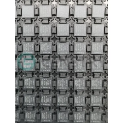
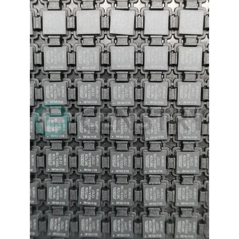
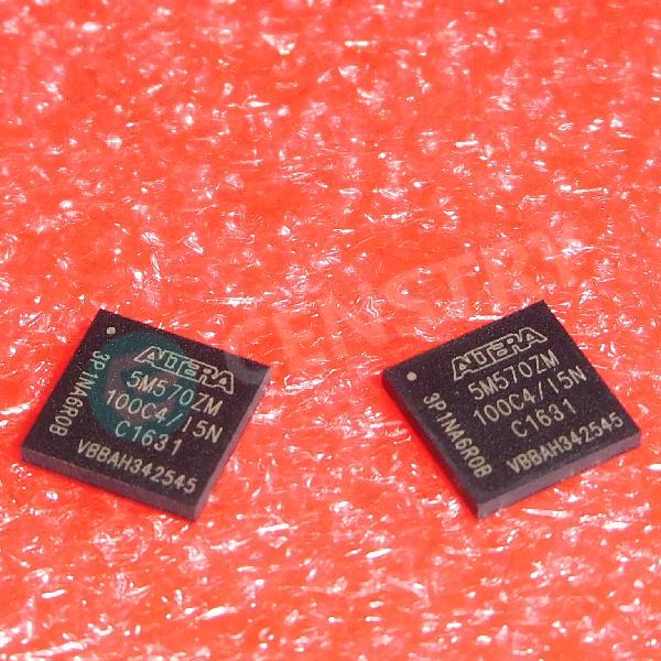
CPLD - Complex Programmable Logic Devices CPLD - MAX V 440 Macro 74 IOs


Les images sont fournies à titre indicatif.
Voir les spécifications du produit pour plus de détails sur le produit.
CPLD - Complex Programmable Logic Devices CPLD - MAX V 440 Macro 74 IOs
Les commandes de plus de 200 $ sont éligibles pour un cadeau de style chinois en édition limitée.
Les commandes de plus de 1 000 $ bénéficient d'une dispense des frais d'expédition de 30 $..
Les commandes supérieures à 5 000 $ bénéficient d'une exemption des frais d'expédition et de transaction..
Ces offres sont applicables aux nouveaux clients et aux clients existants et sont valables du 1er janvier 2024 au 31 décembre 2024..
Altera
5M570ZM100I5N datasheet
MBGA100
Puces IC
 Lead free/RoHS Compliant
Soumettez votre demande de devis maintenant et nous espérons vous fournir un devis dans les délais juin 30, 2024. Passez votre commande maintenant et nous prévoyons de finaliser la transaction dans les juillet 04, 2024. Ps : L’heure est conforme à GMT+8h00.


Feature
The following list summarizes the MAX V device family features:
■ Low-cost, low-power, and non-volatile CPLD architecture
■ Instant-on (0.5 ms or less) configuration time
■ Standby current as low as 25 µA and fast power-down/reset operation
■ Fast propagation delay and clock-to-output times
■ Internal oscillator
■ Emulated RSDS output support with a data rate of up to 200 Mbps
■ Emulated LVDS output support with a data rate of up to 304 Mbps
■ Four global clocks with two clocks available per logic array block (LAB)
■ User flash memory block up to 8 Kbits for non-volatile storage with up to 1000 read/write cycles
■ Single 1.8-V external supply for device core
■ MultiVolt I/O interface supporting 3.3-V, 2.5-V, 1.8-V, 1.5-V, and 1.2-V logic levels
■ Bus-friendly architecture including programmable slew rate, drive strength, bus-hold, and programmable pull-up resistors
■ Schmitt triggers enabling noise tolerant inputs (programmable per pin)
■ I/Os are fully compliant with the PCI-SIG® PCI Local Bus Specification, revision 2.2 for 3.3-V operation
■ Hot-socket compliant
■ Built-in JTAG BST circuitry compliant with IEEE Std. 1149.1-1990
Functional Description
MAX V devices contain a two-dimensional row- and column-based architecture to implement custom logic. Row and column interconnects provide signal interconnects between the logic array blocks (LABs).
Each LAB in the logic array contains 10 logic elements (LEs). An LE is a small unit of logic that provides efficient implementation of user logic functions. LABs are grouped into rows and columns across the device. The MultiTrack interconnect provides fast granular timing delays between LABs. The fast routing between LEs provides minimum timing delay for added levels of logic versus globally routed interconnect structures.
The I/O elements (IOEs) located after the LAB rows and columns around the periphery of the MAX V device feeds the I/O pins. Each IOE contains a bidirectional I/O buffer with several advanced features. I/O pins support Schmitt trigger inputs and various single-ended standards, such as 33-MHz, 32-bit PCI™, and LVTTL.
MAX V devices provide a global clock network. The global clock network consists of four global clock lines that drive throughout the entire device, providing clocks for all resources within the device. You can also use the global clock lines for control signals such as clear, preset, or output enable.

Request a quote 5M570ZM100I5N at censtry.com. All items are new and original with 365 days warranty! The excellent quality
and guaranteed services of 5M570ZM100I5N in stock for sale, check stock quantity and pricing,
view product specifications, and order contact us:sales@censtry.com.
The price and lead time for 5M570ZM100I5N depending on the quantity required, please send your request to us,
our sales team will provide you price and delivery within 24 hours, we sincerely look forward to cooperating with you.
Altera
4000 PCS
EP4CE15E22C8N .PDF
Altera
1 PCS
EP3C16E144I7N .PDF
Altera
2000 PCS
EPM240T100I5N .PDF
Altera
2470 PCS
ES1030QI .PDF
2024-06-29
WORKING GOOD
2024-06-29
buen producto rapida entrega
2024-06-29
thanks so much
2024-06-29
very fast tony


Nous apprécions grandement vos commentaires. Veuillez partager votre avis le plus authentique.
*Veuillez vous connecter à votre compte avant de publier un commentaire